ATCA-PTSW-AMC4
Table of contents
- 1. DATASHEET
DATASHEET
The ATCA-PTSW-AMC4 board (Pcie and Timing SWitch with 4 AMC slots) is a cutaway quad-AMC module carrier, compliant with the ATCA (PICMG 3.0) specification and compatible with the ATCA extension for Physics (PICMG 3.8 ARTM). Most mid/full-size AMC modules available from industry can be installed in the board.
Details can be found on the User Manual.
The board main charateristics are summarized below.
PCI Express switch
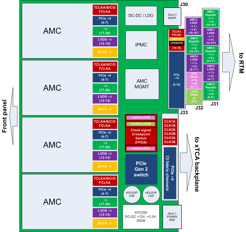
PCIe data switching performed by a PLX PEX8696 (PCIe Gen 2), which interconnects:
- 13 fabric channels (×4 links), connecting up to the other 13 PCI Express (PICMG 3.4 R1.0) compliant modules
- 4 AMC modules (four ×4 PCIe links - AMC.1 R2.0)
- 1 RTM module (one ×16 PCIe link)
- Onboard FPGA (one ×4 PCIe link, PCI Express® External Cabling R1.0.)
Any of the PCIe links listed is settable as "upstream" (where the PCIe host is connected).
Clock/timing distribution crosspoint-switch
The ATCA, AMC and RTM timing/clock lines are managed and routed by a crosspoint-switch implemented on a Virtex-6 FPGA, which:
- Distributes clocking and synchronization signals to/from compliant AMC/RTM inserted modules.
- Interfaces to ATCA clock and synchronization bus: for clock distribution to compliant modules within the shelf.
- Routes any clock signal source from any of the AMCs, from the RTM, from the ATCA backplane or even locally generated in the FPGA, to any synchronization input.
- Other external synchronization signals may be input through the RMC module on the RTM card. Currently, IEEE-1588-2008 and standard TTL clock/trigger sync interfaces are available.
| AMC/RTM clock lines | function | ATCA "clock & sync" |
|---|---|---|
| TCLKA (slot 2) or TCLKB (slot 1) | synchronization clock (100MHz) | CLK1A (slot 2) or CLK1B (slot 1) |
| TCLKC (slot 2) or TCLKD (slot 1) | absolute time (IRIG-B) | CLK2A (slot 2) or CLK2B (slot 1) |
| FCLKA | PCIe reference clock | CLK3A (slot 2) or CLK3B (slot 1) |
(Correspondance between "ATCA clock and synchronization interface" and AMC/RTM clock lines and respective function (middle column). "slot 1" / "slot2" indicates that the particular signal is active when the ATCA-PTSW-AMC4 front board is inserted in slot 1 / slot 2.)
Rear Transmission Module
The rear transmission module is compatible with the PICMG 3.8 (ARTM, "Zone 3A") standard. The card provides digital connectivity on the back-panel of the ATCA shelf and contains the following interfaces:
- PCI Express over-cable iPass™ connector (16× link)
- Ethernet port on SFP connector (1× link) connected to the AMC1 slot .
- External Timing module mezzanine: such as RMC-TMG-1588 (IEEE-1588-2008 over Ethernet sync to an external Grand Master Clock).
- Four SFP connectors (x1 each), connected to the FPGA’s MGT transceivers; furthermore, 8 LVDS pairs from the FPGA are connected to the SFP transceiver control lines (2 pairs/SFP).
- One x4 RapidIO channel and 8 LVDS pairs connected to each AMC slot are also available for future expansion.
Other interfaces
- CoreIPM OPMA2368 IPM Controller
- Serial EEPROM for PEX 8696 configuration
Figure 1 - Board interfaces.

Multi-processor configurations
The following figure shows a configuration where an ATCA-PTSW-AMC4 card is configured as a 5-virtual-switch hub (SW-H). Each PCIe virtual switch circuit connects 3 node cards (1 card on VC3) where one is an ATCA-PTSW-AMC4 card configured as a processor carrier node card (SW-N) (except on VC3). This card can connect up to 5 processors (4 AMC, 1 external - PCIe Cable) where only one is configured as PCIe Upstream.
SW-H and SW-N will differ only on the PCIe switch programming (PLX PEX8696), which may be fixed (2 different board types) or eventually field programmed through the IPMC. No modifications to the DAQ cards are required.
Figure 2 - Five ATCA-PTSW-AMC4 cards using 5 PCIe switch virtual channels.
Other possible configurations are:
- 7 virtual switches each with 7 x [1 PTSW + 1 DAQ card].
- 5 (4+1) virtual switches with 4 x [1 PTSW + 2 DAQ cards] and 1 x [1 PTSW + 1 DAQ cards].
- 3 (2+1) virtual switches with 2 x [1 PTSW + 4 DAQ cards] and 1 x [1 PTSW + 3 DAQ cards].
An alternative configuration:
- Use just 1 ATCA-PTSW-AMC4 card configured for 3 virtual switches on Slot 1.
- Insert 2 AMC processor cards + 1 external PCIe cable computer to the PTSW card.
- Each processor controls up to 4 DAQ cards for a grand total of 12.
Figure 3 - Block diagram of the board.


